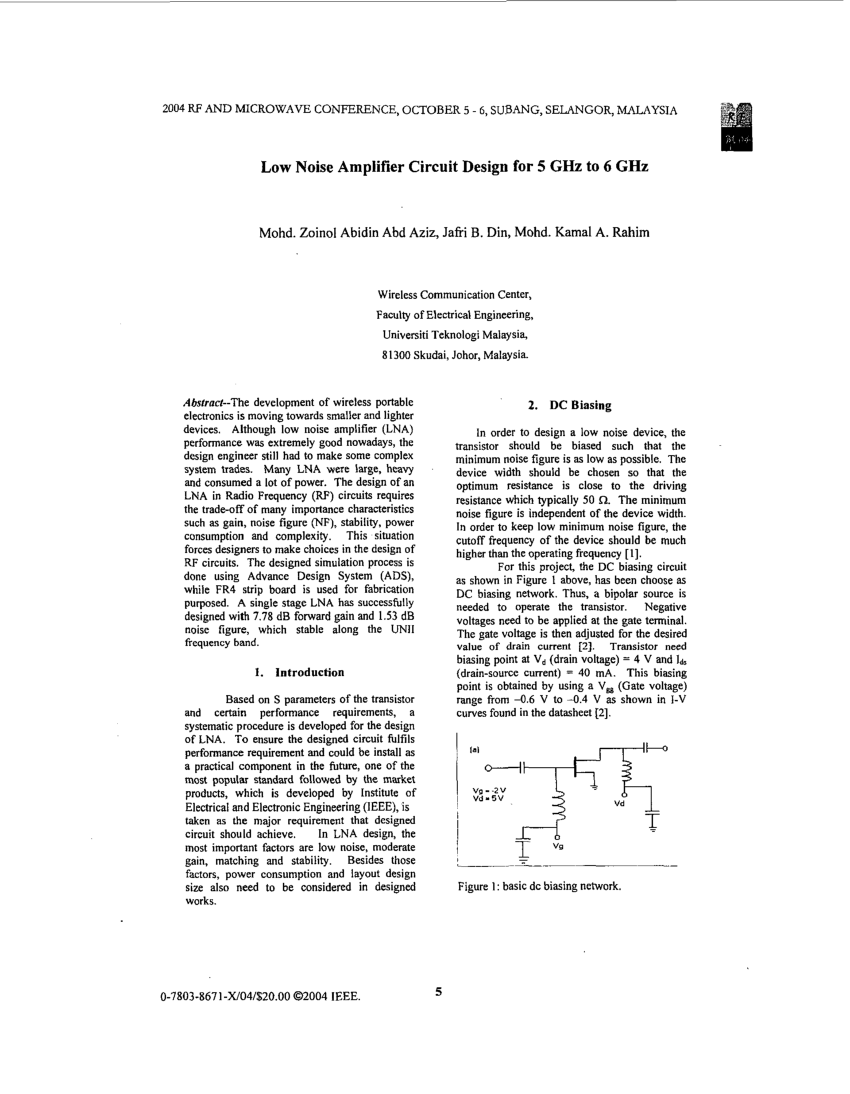
PDF Low noise amplifier circuit design for 5 GHz to 6 GHz Circuit Diagram Many transistors have been measured and modeled for the source impedance that yields the lowest noise - measured by the noise figure (NF). The noise factor, F, is the ratio of the signal to noise ratio of the input to the signal to noise ratio of the output, NF is 10log 10 F. Noise figure (NF) is always greater than zero. Figure 2(c) shows
A Low Noise Amplifier (LNA) is an electronic amplifier designed to boost very weak RF signals while adding as little additional noise as possible (Low-noise amplifier - Wikipedia).In a receiver chain, the LNA is typically the first active component after the antenna (FAQ | ShareTechnote).Its primary role is to increase the signal strength of faint incoming radio signals to a level suitable

Designing and testing a low Circuit Diagram
#62 In this electronics tutorial mini-series I set out to build a low noise signal amplifier to measure very small signals that are usually below the generic ECE145A/ECE218A Design of Low Noise Amplifiers Design of Low Noise Amplifiers We have already studied amplifier design for stability gain Now we will consider how to design for lowest noise. Recall 2 3 1 112 1 1 total F F FF GGG − − =+ + +" • The noise factor of the first stage, F1, dominates the overall noise performance if G1 is

A Low Noise Amplifier (LNA) is an RF amplifier designed to boost very weak signals without significantly degrading the signal-to-noise ratio (SNR). These amplifiers operate in the front-end of communication receivers, positioned immediately after the antenna, to ensure that weak signals are strong enough for further amplification and processing. For someone into HAM radio, you might have come across weather satellite LRPT reception using an RTL-SDR. Receiving images from a satellite may require a good low-noise amplifier. On the other hand, someone into radio astronomy definitely requires a very low noise amplifier to receive the hydrogen line frequency emanating from the milky way.
PDF Design of Low Noise Amplifiers Circuit Diagram
• NFsys is the cascaded noise figure of the system referred to the input (the Friis formula). • Fn and Gn are the noise factor and linear gain, respectively, of each successive stage within the receiver signal chain. • Prin is the noise floor for receiver input sensitivity. • kT is thermal noise density: -174 dBm/Hz at room temperature
